又是發售前情報…. 最近非常確實地體感到網路小道的發達….
http://www.neogaf.com/forum/showthread.php?t=203994
20GB/60GB North American Launch:
Has PS2 CPU and GPU hardware60GB PAL Launch / 80GB US:
Has PS2 GPU hardware40GB 65nm motherboard:
Has no PS2 hardwareEngadget:
-65nm
-Reduced the power usage to around 135 Watts from 200 Watts.
-Runs cooler and quieter
-Smaller heat pipe-PS2 hardware was located on the left side of the motherboard.
-Board width is approximately 15% shorter in the 65nm version.
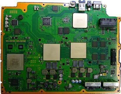
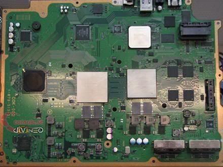
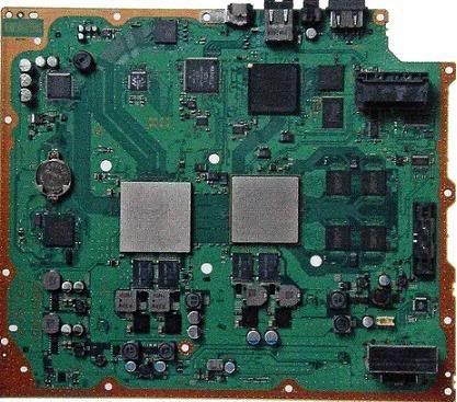
此外,因為PS2晶片全面移除,PCB整個縮小了約1/8左右,同時影響到散熱器的位置與規模。
和有變動的CELL供電迴路相比,RSX的供電迴路並沒有變動,應該是維持90nm沒有修改,未來應該還有再抑制發熱量的機會。
[EDIT]
http://ps3.qj.net/Sony-new-40GB-PS3-still-using-90nm-chips/pg/49/aid/106762
和ITmedia相同,SONY表明是維持90nm CELL。
[EDIT2]
http://pocketnews.cocolog-nifty.com/pkns/2007/11/40gbps340gbps3_d791.html
歐洲的40GB與日本的40GB不同?
20GB/60GB North American Launch:
Has PS2 CPU and GPU hardware60GB PAL Launch / 80GB US:
Has PS2 GPU hardware40GB 65nm motherboard:
Has no PS2 hardwareEngadget:
-65nm
-Reduced the power usage to around 135 Watts from 200 Watts.
-Runs cooler and quieter
-Smaller heat pipe-PS2 hardware was located on the left side of the motherboard.
-Board width is approximately 15% shorter in the 65nm version.
此外,因為PS2晶片全面移除,PCB整個縮小了約1/8左右,同時影響到散熱器的位置與規模。
和有變動的CELL供電迴路相比,RSX的供電迴路並沒有變動,應該是維持90nm沒有修改,未來應該還有再抑制發熱量的機會。
[EDIT]
http://ps3.qj.net/Sony-new-40GB-PS3-still-using-90nm-chips/pg/49/aid/106762
和ITmedia相同,SONY表明是維持90nm CELL。
[EDIT2]
http://pocketnews.cocolog-nifty.com/pkns/2007/11/40gbps340gbps3_d791.html
歐洲的40GB與日本的40GB不同?
[EDIT3]
各區域40GB PS3情報確認:
歐洲-G04,90nm
日本-H00,65nm
美國-G01跟H01,G01是90nm,H01是65nm
所以SCEE說40GBPS3為90nm是正確的,只是只適用於歐洲。
CECH
00 日本 A00 B00 H00
01 USA A01 B01 E01 G01 H01
02 オーストラリア/ニュージーランド C02
03 イギリス/アイルランド C03
04 ヨーロッパ/中東/アフリカ C04
05 韓国 E05 G05
06 香港 E06
07 台湾 A07 B07
08 ロシア/インド C08
A0x 60GB
B0x 20GB 無線LAN、メモカ無し
C0x 60GB GS無し
E0x 80GB GS無し
G0x 40GB PS2、メモカ無し USB*2 5.0kg
H0x 40GB PS2、メモカ無し USB*2 4.4kg